
Introduction
In 3D packaging, there exists a fundamental technical contradiction: the higher the interconnect density, the smaller the bump pitch, and the less reliable traditional solder bumps become. When the pitch is compressed below 10μm, the surface tension of molten solder causes bridging short circuits.
Meanwhile, the solder layer itself, with its height of tens of micrometers, introduces additional resistance, capacitance, and thermal resistance. The growth of parasitic parameters directly consumes the benefits of performance improvements. Taking High Bandwidth Memory (HBM) as an example, its interconnect structure is shown in Figure 1. From the figure, it can be clearly seen that microbumps and the underfill layer constitute the main height source of the vertical channel. As the number of stacked layers climbs above 12Hi, the bottlenecks of this structure in terms of parasitic effects, heat dissipation, and mechanical warpage become increasingly prominent.
The current mainstream HBM3E still adopts the microbump plus underfill solution, with single-stack bandwidth of approximately 1.2 TB/s (HBM3 is 819 GB/s), and the aggregate bandwidth of flagship AI accelerator cards has reached the 8TB/s level. As stacking advances from 12Hi to 16Hi and beyond, the height, heat dissipation, and warpage of microbumps are approaching the physical limits of this route.
The solution to resolve this contradiction is to completely eliminate bumps and solder, allowing the copper electrodes of two wafers to contact "face-to-face" directly. This is the core concept of Hybrid Bonding: achieving wafer pre-bonding at room temperature through atomic-level planarization and surface activation, followed by annealing to simultaneously form copper-copper metallic bonding and oxide covalent bonding sealing.
It completes both metal interconnection and dielectric sealing in one step, opening a new technical path for three-dimensional chip stacking in the post-Moore era. This article will progressively disassemble how this path is realized, from technical principles, core process chains, to mass production routes.
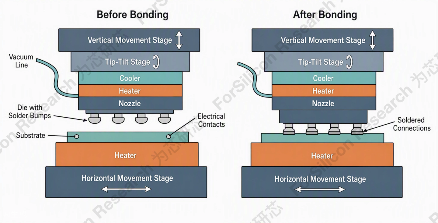
Figure 1 Schematic diagram of microbump interconnect structure (Image source: Coherent)
Technical Principles
1.1 The Meaning of "Hybrid"
"Hybrid" refers to the simultaneous completion of metallic bonding and dielectric bonding at the same interface and in the same annealing step.
Specifically, copper electrodes achieve metallic bonding through atomic thermal diffusion, forming low-resistance conductive pathways; simultaneously, hydroxyl groups on the surface of silicon dioxide and other oxide dielectric layers undergo dehydration condensation, forming Si-O-Si covalent bonds, achieving permanent fusion and sealing of the dielectric layer. Metal interconnection is responsible for electrical performance, while dielectric bonding is responsible for mechanical strength and environmental isolation—neither can be omitted, together forming the physical foundation of hybrid bonding.
1.2 Differences from Traditional Bonding
First, no solder layer: traditional solutions rely on tin-based solder or microbumps as connection media, with a third material present at the interface; hybrid bonding completely eliminates bumps, with copper electrodes contacting "face-to-face" directly.
Second, room-temperature pre-bonding: thermocompression bonding requires alignment at high temperature and high pressure, with thermal expansion mismatch easily causing offset; hybrid bonding first achieves initial bonding and locking through hydrogen bonds between surface hydroxyl groups at room temperature, with annealing used only for curing—no thermal stress alignment throughout the process.
Third, atomic-level contact: traditional bonding relies on solder to form metallurgical connections, not requiring atomic-level fit at the interface; whereas hybrid bonding requires large-area atomic-level direct contact between copper surfaces and oxide surfaces, with interface resistance and thermal resistance therefore significantly reduced.
Core Process Chain
2.1 Prerequisite Foundation: TSV, Copper Filling, and Wafer Thinning
Hybrid bonding does not occur from nothing—it requires copper electrodes and clean dielectric layers on the wafer surface for bonding. In 3D stacking scenarios requiring vertical interconnection, high-aspect-ratio through-silicon vias (TSV, see Figure 2) must first be etched into the silicon wafer.
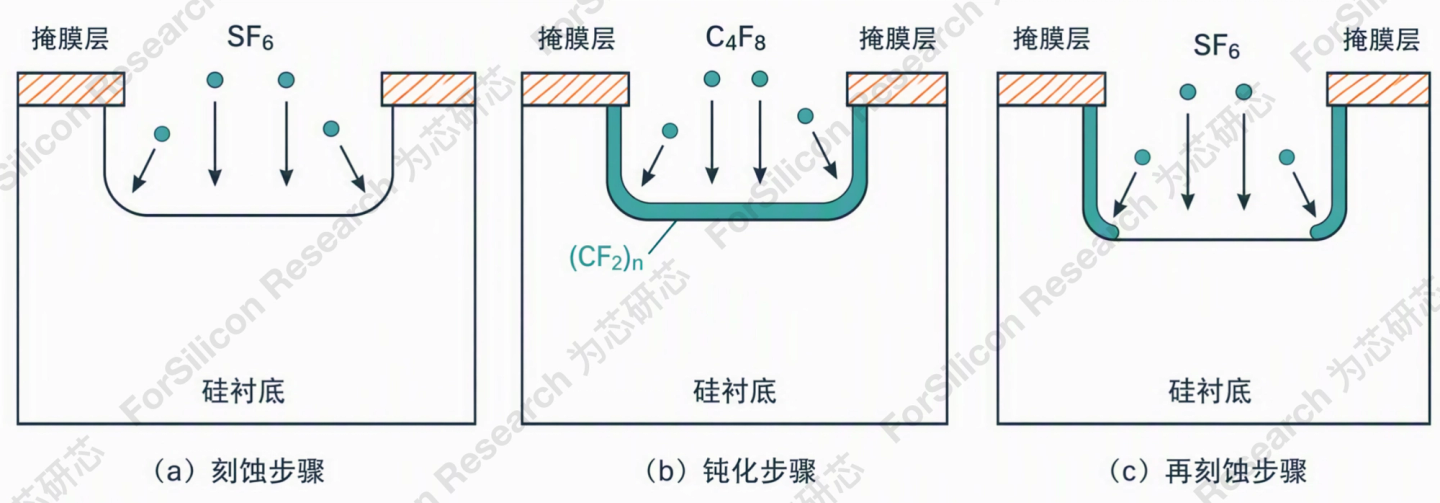
Figure 2 Schematic diagram of TSV process (Image source: ForSilicon Research)
Through insulating layer deposition, barrier layer, seed layer sputtering, and copper electroplating filling, copper conductive pillars are formed within the vias (Figure 3).
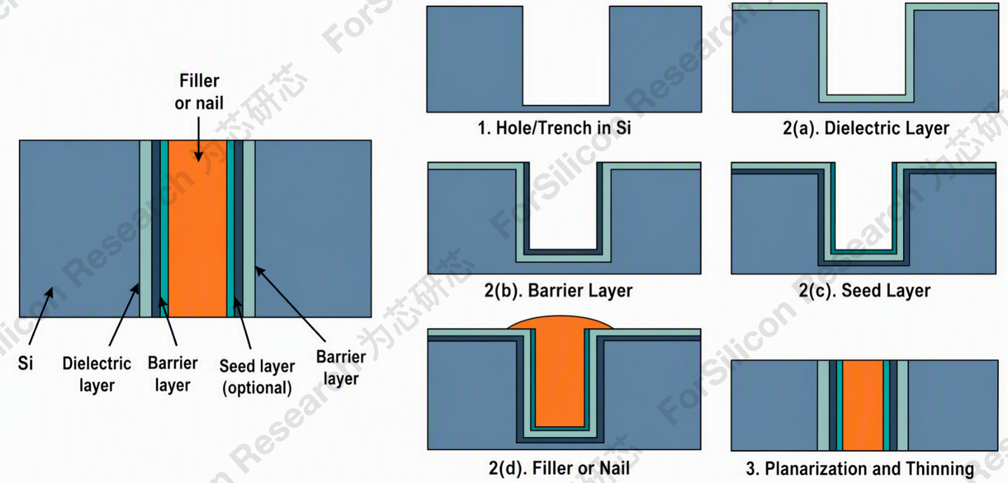
Figure 3 Copper filling process flow diagram (Image source: ForSilicon Research)
Subsequently, the wafer is thinned from the original hundreds of micrometers thickness to the tens of micrometers range. After back-side grinding and chemical mechanical polishing (CMP), the front side has flat copper pads and oxide dielectric surfaces, while the back side exposes the copper electrodes at the bottom of the TSV, creating the most basic physical conditions for hybrid bonding.
2.2 Surface Precision Control: CMP and Copper Dishing Management
Hybrid bonding has extremely demanding requirements for surface flatness. In the final CMP step, copper and silicon dioxide are simultaneously polished to atomic-level flatness. However, copper's hardness is far lower than that of oxide, and during polishing it is easily over-polished, forming nanometer-scale copper dishing (see Figure 4).
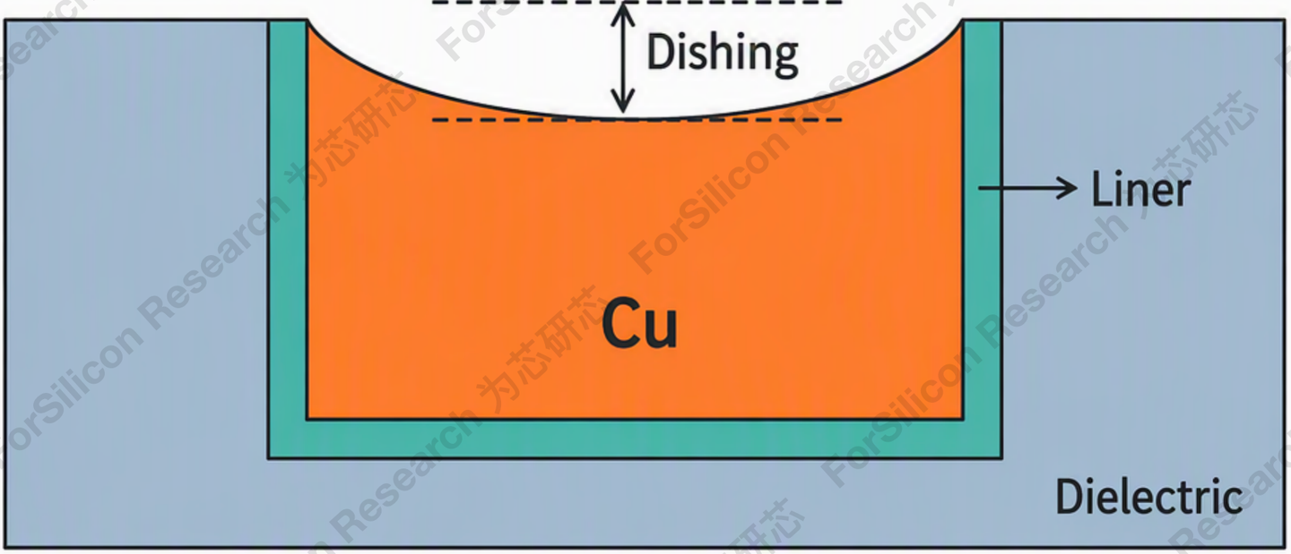
Figure 4 Schematic diagram of copper dishing (Image source: Vetek)
This dishing is not a defect, but rather a process window that needs to be controlled: the typical target value is around 3-5nm. The reason is that during subsequent annealing, copper's thermal expansion coefficient is significantly higher than the surrounding oxide, and the copper regions will thermally expand upward. If the dishing is properly controlled during the CMP stage, the copper expansion during annealing will exactly fill the dishing, allowing both copper surfaces to achieve atomic-level coplanar contact; if the dishing is too deep or too shallow, it will cause contact voids or extrusion overflow, directly determining the bonding resistance and reliability.
2.3 Surface Chemical Activation: From Cleaning to Hydroxylation
After CMP, the wafer enters a vacuum plasma chamber for surface activation. High-energy plasma, through physical sputtering, removes organic contaminants and nanometer-scale particles adsorbed on the surface, achieving atomic-level cleanliness; simultaneously, active particles in the plasma strike the silicon dioxide surface, breaking Si-O-Si bonds and producing numerous silicon dangling bonds (Figure 5), causing the originally stable tetrahedral network structure to form high-energy active sites on the surface.
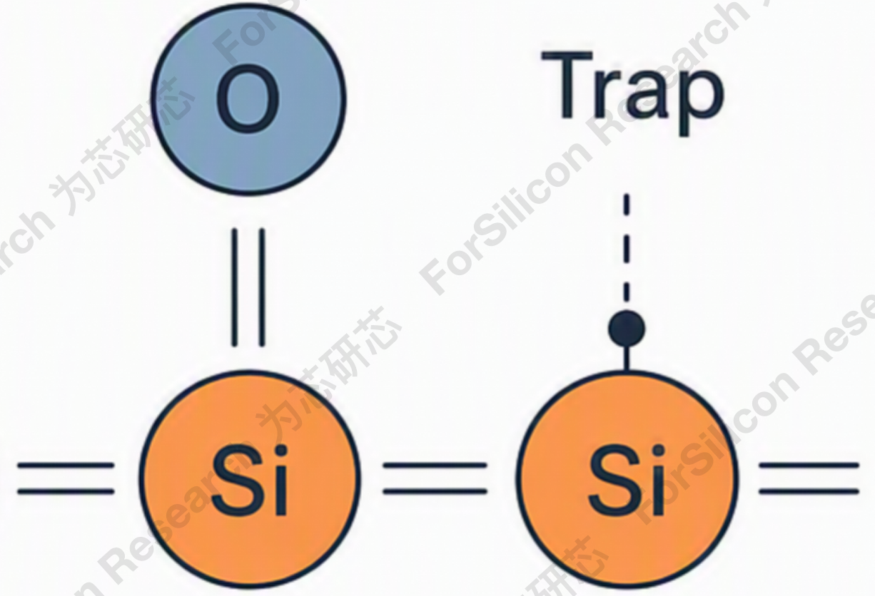
Figure 5 Atomic structure diagram of silicon dangling bonds (Image source: ForSilicon Research)
The activated wafer is immediately cleaned with ultra-pure water (resistivity 18.2 MΩ·cm). When water molecules contact these high-energy dangling bonds, dissociative adsorption occurs—the water molecules are dissociated and form a high density of silanol groups (Si-OH) on the surface. The entire silicon dioxide surface thereby transforms from a hydrophobic state to a super-hydrophilic state, covered with hundreds of millions of hydroxyl groups (Figure 6). This step is the chemical foundation for subsequent bonding, providing sufficient hydrogen bond adhesion.
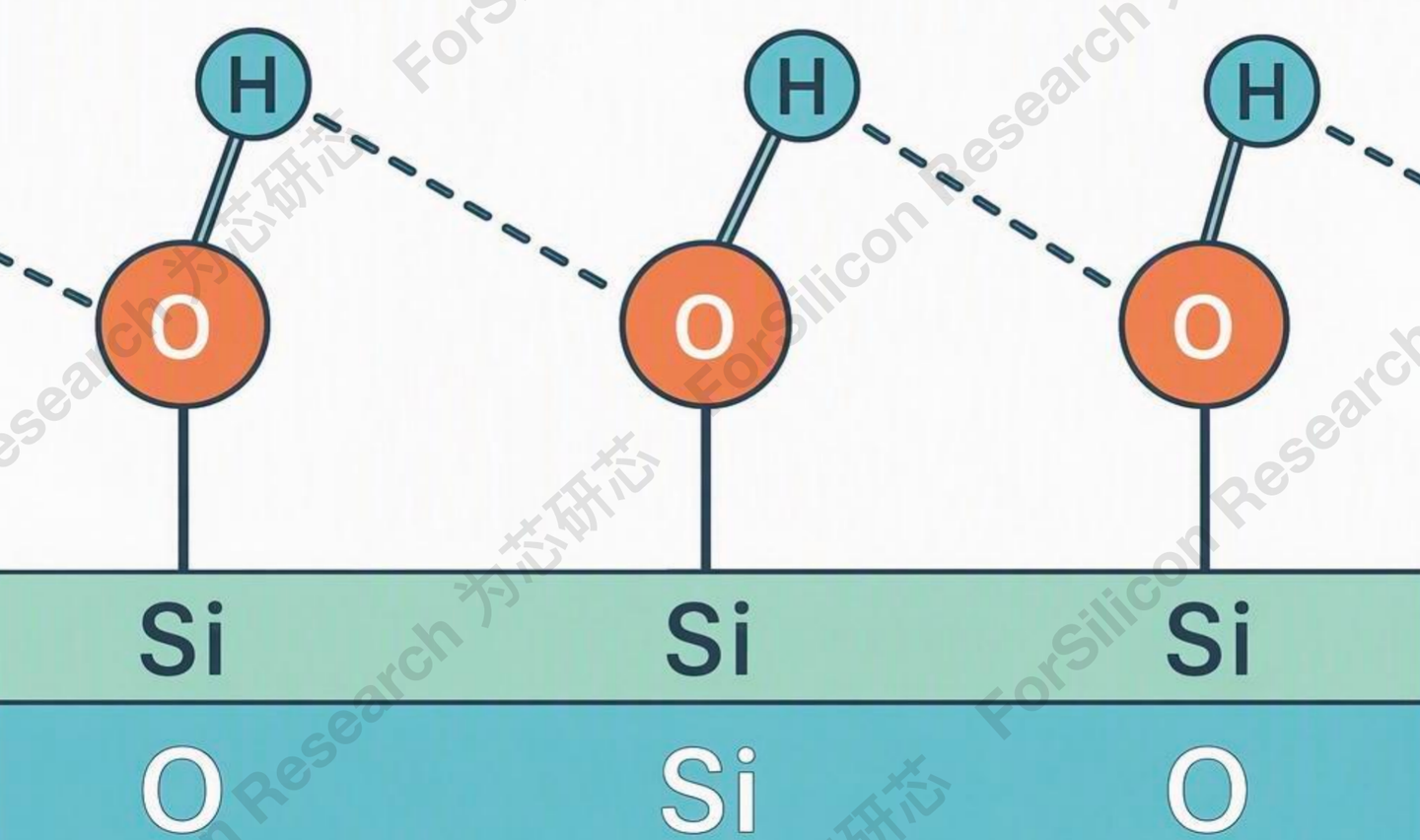
Figure 6 Schematic diagram of hydrogen bonds between SiO₂ surface hydroxyl groups (Image source: ForSilicon Research)
2.4 Room-Temperature Pre-Bonding: The Temporary Lock of Hydrogen Bonds
Next, the two processed wafers achieve high-precision alignment under a precision alignment system, then slowly bond at room temperature with very low pressure (see Figure 7).
At this point, the hydroxyl groups on the oxide surfaces of both wafers approach each other, forming hydrogen bond bridges—a surface's hydroxyl hydrogen atoms experience electrostatic attraction with the lone electron pairs of oxygen atoms on the other surface. Although the bond energy of a single hydrogen bond is weak, the simultaneous action of hundreds of millions of hydroxyl groups produces sufficient total adhesion to tightly lock the two wafers at room temperature, preventing slippage or detachment.
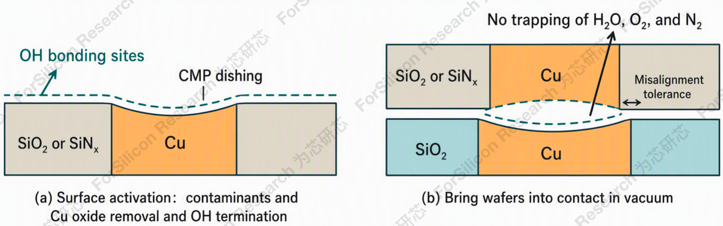
Figure 7 Schematic diagram of pre-bonding (Image source: ForSilicon Research)
The core advantage of this step is low-temperature, stress-free operation—the wafers complete alignment and initial locking at room temperature, completely avoiding the thermal expansion coefficient mismatch problem caused by high-temperature alignment. However, since hydrogen bonds are weak interactions, the wafer pair after pre-bonding still has a risk of debonding if subjected to mechanical disturbance or prolonged storage, so they typically need to be transferred to the annealing process as soon as possible.
2.5 Annealing and Curing: From Temporary Adhesion to Permanent Connection
The pre-bonded wafers are placed in a low-temperature annealing furnace at 200-400°C, where the following two types of permanent bonding reactions will occur simultaneously.
In the dielectric layer, the hydroxyl groups on both silicon dioxide surfaces undergo dehydration condensation reaction: Si-OH combines with HO-Si, releasing water molecules and forming Si-O-Si covalent bonds. The bond energy of covalent bonds is far higher than that of hydrogen bonds, achieving permanent fusion and hermetic sealing of the oxide dielectric layer.
In the metal layer, the copper pads thermally expand, with the upward-bulging portions exactly filling the nanometer-scale dishing controlled during the CMP stage, enabling large-area atomic-level contact between the two copper surfaces. Copper atoms cross the interface through thermal diffusion, forming metallic bonds and constructing low-resistance, high-reliability conductive pathways.
After annealing is complete, both the SiO₂-SiO₂ covalent bonding and Cu-Cu metallic bonding are simultaneously secured, declaring the physical and electrical connections of hybrid bonding complete (Figure 8).
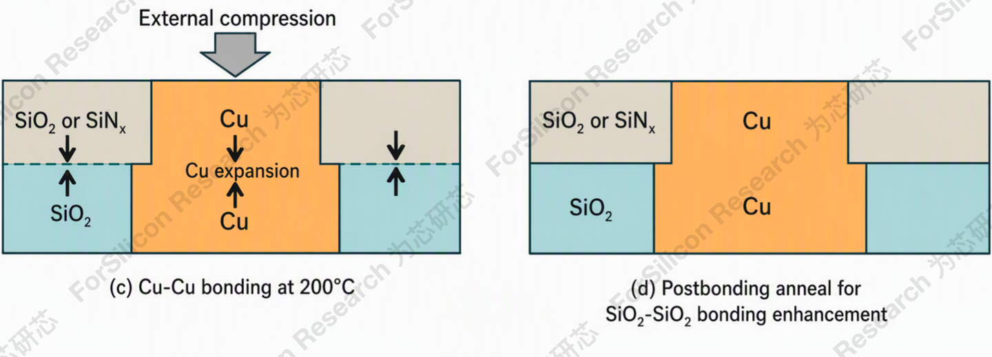
Figure 8 Schematic diagram of annealing and curing (Image source: ForSilicon Research)
Mass Production Routes
3.1 W2W (Wafer-to-Wafer)
W2W directly aligns and bonds two complete wafers, processing the entire wafer at once. Its advantages are mainly reflected in precision and efficiency—alignment precision can reach sub-micron levels or higher, and without the need for dicing, sorting, and pick-and-place of individual dies, throughput is extremely high.
This route has achieved mature mass production in CMOS image sensors (CIS) and 3D NAND. Sony has used W2W hybrid bonding for high-end smartphone CIS since 2015, while Yangtze Memory's Xtacking architecture achieves vertical integration of CMOS and storage layers through W2W.
However, W2W's disadvantages are equally prominent: the two wafers must be exactly the same size, and there is a yield multiplication effect—if one defective die exists on either wafer, the entire bonded pair at that position will be scrapped, therefore requiring both wafers to have extremely high yield levels.
In the HBM field, W2W is regarded as the future direction for homogeneous DRAM die stacking, with its large-scale implementation expected to occur from the HBM4E later generation to the HBM5 generation (approximately 2027-2029). Beyond HBM, W2W has begun penetrating edge-side AI chips—in August 2026, Xiaomi's edge-side AI acceleration chip Xuanjie O100 achieved three-layer wafer stacking using W2W, with bandwidth reaching 1.22TB/s.
3.2 D2W Collective (Die-to-Wafer Collective Bonding)
D2W Collective is an intermediate route between W2W and pure individual die bonding. Dies are first diced and sorted, then placed in batches onto a carrier wafer. The entire carrier wafer and target wafer undergo activation, cleaning, and bonding together, after which the carrier is removed, leaving the bonded dies.
This method leverages the carrier wafer to achieve "batch preprocessing," maintaining some flexibility while significantly improving throughput efficiency compared to individual processing. This route will be mainly applied to SRAM on Logic (stacking SRAM cache on logic chips) and some CIS scenarios.
Its disadvantage lies in the added carrier wafer management and removal steps, and edge contamination after die dicing still needs to be controlled before batch processing.
3.3 D2W Sequential (Die-to-Wafer Sequential Bonding)
D2W Sequential adopts a single-die, layer-by-layer processing approach. Known-good dies after dicing are transferred one by one, and after activation and cleaning, are directly picked up and placed onto the target wafer by a high-precision bonder tool. This is the route with outstanding flexibility—capable of mixing dies of different sizes, different process nodes, or even different materials—it is the key path to achieving Chiplet heterogeneous integration.
Currently, the interconnect pitch baseline for D2W mass production is still at the 9μm level, with the industry pushing toward 3μm and even 1μm. At ECTC 2026, CEA-Leti demonstrated 1μm pitch D2W hybrid bonding for the first time, though yield is still limited by the alignment precision of existing equipment.
However, this route faces severe challenges: micro-cracks and organic contamination exist at die dicing edges, probe testing damages the copper pad surface, requiring additional repair processes; coupled with the die-by-die processing flow, the bonding step becomes the slowest and most expensive link in the entire process chain.
In the HBM field, D2W Sequential mainly targets heterogeneous integration scenarios for logic base die and DRAM stacking, representing one of the important technology options for HBM4E later generation and subsequent generations.
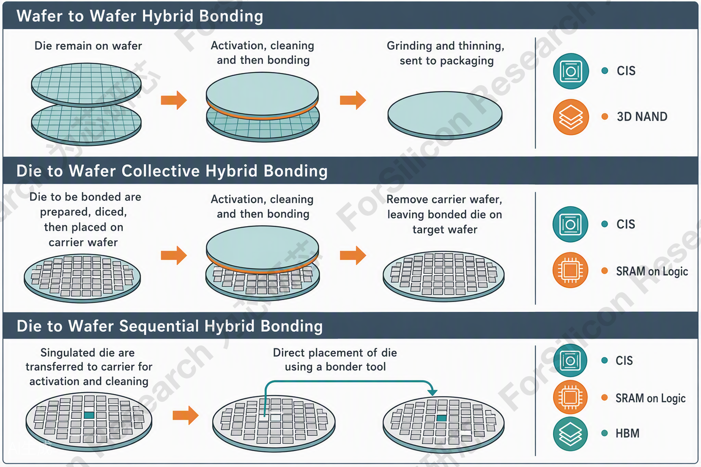
Figure 9 W2W & D2W comprehensive comparison chart (Image source: SemiAnalysis & KLA)
Conclusion
Hybrid bonding has achieved mature mass production in CMOS image sensors and has established application foundations in 3D NAND (such as Yangtze Memory's Xtacking).
In August 2026, Xiaomi released its edge-side AI acceleration chip Xuanjie O100, using W2W hybrid bonding with three-layer wafer stacking (2 layers of DRAM + 1 layer of NPU), achieving 1.22TB/s bandwidth. The chip has completed tape-out verification and is planned for mass production in 2027, marking a key step for hybrid bonding moving from cloud-side AI accelerators to edge-side AI devices.
On the HBM side, the approach is more cautious. HBM4 and HBM4E are expected to continue with microbump plus underfill as the mainstream solution. The introduction timing for hybrid bonding in HBM may fall in the HBM4E later generation to HBM5 generation; at that point, facing 16Hi and above stacking and I/O density multiplication, hybrid bonding will become a key technology. Additionally, packaging-level thermal dissipation innovations such as Samsung's HPB and SK Hynix's iHBM are also sharing the bottleneck pressure of traditional solutions.
From CIS, 3D NAND to HBM and edge-side AI, the physical limits encountered by microbumps are being progressively dismantled by hybrid bonding through "copper-to-copper direct connection." The three routes of W2W, D2W Collective, and D2W Sequential will also evolve in parallel across different scenarios for the long term. This rewriting of vertical interconnect density has just begun.
About ForSilicon Research. ForSilicon Research focuses exclusively on China's semiconductor equipment, materials, and components — delivering primary-research data and long-term value insight for enterprises and investors. Learn more →